Communication Protocols on STM32 (Part 2): SPI – the four CPOL/CPHA modes and reading W25Qxx flash
SPI on STM32, from the shift-register principle and the four CPOL/CPHA modes to SCK speed per prescaler and reading the ID, reading, erasing and programming W25Qxx flash with HAL and DMA. Part 2 of the Communication Protocols on STM32 series.
Note: the diagrams in this article were drawn by Capitlab for illustration. Table values are calculated from formulas; the "Measured" column will be filled in once measurements are made on hardware. The code was written from the HAL documentation and datasheets and has not yet been run on hardware, so verify it before using it in a product.
SPI (Serial Peripheral Interface) shows up in flash chips, SD cards, displays, ADCs and IMU sensors. It is much faster than UART or I²C, but it needs more wires and has no built-in acknowledge (ACK) or error detection. If the slave does not answer, the master still reads back a stream of bytes; they are just wrong.
When SPI "doesn't work", the most common cause is the wrong CPOL/CPHA mode, followed by releasing chip select too early. This part explains both, then uses a Winbond W25Qxx flash to read the ID and to read, erase and program data.
1. How it works
SPI has one master and one or more slaves, using four signals:
| Signal | Direction | Meaning |
|---|---|---|
| SCK | Master → Slave | Clock generated by the master |
| MOSI | Master → Slave | Data from the master (Master Out, Slave In) |
| MISO | Slave → Master | Data from the slave (Master In, Slave Out) |
| CS (or NSS) | Master → Slave | Slave select, active low |
Think of the master and slave as one ring of shift registers. On every SCK pulse the master pushes one bit out on MOSI and at the same time takes one bit in from MISO. Sending and receiving therefore always happen together. To read a byte from a slave, the master has to send a byte of its own (usually 0xFF or 0x00) just to generate 8 clock pulses.
The four SPI modes
Two parameters decide how both sides interpret the clock:
- CPOL (clock polarity) is the idle level of SCK: 0 is low, 1 is high.
- CPHA (clock phase) is the edge used for sampling: 0 is the first edge of the pulse, 1 is the second.
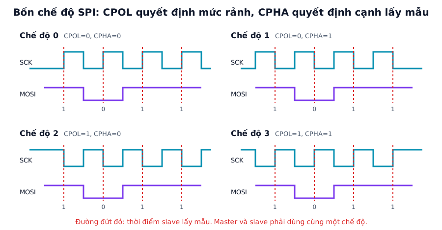
Figure 1. The four SPI modes sending the bits 1, 0, 1, 1. The red dashed lines are where the slave samples, and the data is always stable there. Labels in the figure are in Vietnamese.
| Mode | CPOL | CPHA | SCK idle | Sample on | Data changes on |
|---|---|---|---|---|---|
| 0 | 0 | 0 | Low | Rising edge | Falling edge |
| 1 | 0 | 1 | Low | Falling edge | Rising edge |
| 2 | 1 | 0 | High | Falling edge | Rising edge |
| 3 | 1 | 1 | High | Rising edge | Falling edge |
The required mode is always in the device datasheet. The W25Qxx and many IMU sensors accept both mode 0 and mode 3, but some devices only work in mode 1 or 2. While you are there, check the bit order (MSB first for most parts) and the maximum clock rate.
2. SCK speed on STM32
SCK is the SPI bus clock divided by a prescaler (2, 4, 8, ... 256), so only a handful of discrete values are available. The table is calculated for SPI1 on an 84 MHz bus. These are calculated values, not measurements:
| Prescaler | SCK | Time per byte | Read 4 KB (clock only) | Theoretical throughput |
|---|---|---|---|---|
| 2 | 42 MHz | 0.19 µs | 0.78 ms | 5.25 MB/s |
| 4 | 21 MHz | 0.38 µs | 1.56 ms | 2.63 MB/s |
| 8 | 10.5 MHz | 0.76 µs | 3.12 ms | 1.31 MB/s |
| 16 | 5.25 MHz | 1.52 µs | 6.24 ms | 656 KB/s |
| 32 | 2.625 MHz | 3.05 µs | 12.5 ms | 328 KB/s |
| 64 | 1.3125 MHz | 6.10 µs | 25.0 ms | 164 KB/s |
| 128 | 656 kHz | 12.2 µs | 49.9 ms | 82 KB/s |
| 256 | 328 kHz | 24.4 µs | 99.9 ms | 41 KB/s |
Real throughput is always lower: there is the command and address phase, gaps between bytes when polling, and CPU time. Section 8 will measure the real numbers.
The maximum speed is a limit of the whole circuit, not just the chip. On a breadboard or with long wires, SPI can fail at a few MHz, so start slow and work up. SPI is meant for connections on the same board or a few tens of centimetres. For longer runs, slow down or use a differential bus such as RS-485 or CAN.
3. Wiring
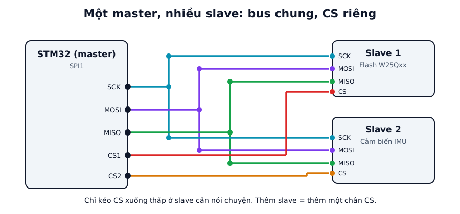
Figure 2. One master, two slaves. SCK, MOSI and MISO are shared; each slave has its own CS pin.
SCK, MOSI and MISO are shared and every slave gets its own CS pin. CS must be high (not selected) from power-up, so set its initial level to High in CubeMX.
The MISO pin of an unselected slave must be high-impedance (Hi-Z). A device that does not release the line will fight the bus and corrupt the other slaves' data.
For wires longer than a few centimetres, put a small series resistor (about 22 to 100 Ω) close to the driving pin to reduce ringing. The boards must share GND and use compatible logic levels.
4. Configuration in STM32CubeIDE
| Setting | Value | Note |
|---|---|---|
| Mode | Full-Duplex Master | |
| Hardware NSS Signal | Disable | Drive CS from a GPIO |
| Data Size | 8 Bits | |
| First Bit | MSB First | Per the datasheet |
| Prescaler | As needed | See the table in section 2 |
| CPOL / CPHA | Per the datasheet | W25Qxx mode 0: Low / 1 Edge |
| CS pin | GPIO Output, initial level High | Label it FLASH_CS |
| DMA | SPI1_TX and SPI1_RX, Normal |
Only when using DMA |
In CubeMX, mode 0 is "Clock Polarity: Low" with "Clock Phase: 1 Edge". Mode 3 is "High" with "2 Edge".
5. Source code
5.1. Reading the W25Qxx JEDEC ID
Command 0x9F returns 3 bytes: manufacturer, memory type and capacity. Winbond's manufacturer code is 0xEF. A W25Q64 returns EF 40 17 and a W25Q128 returns EF 40 18.
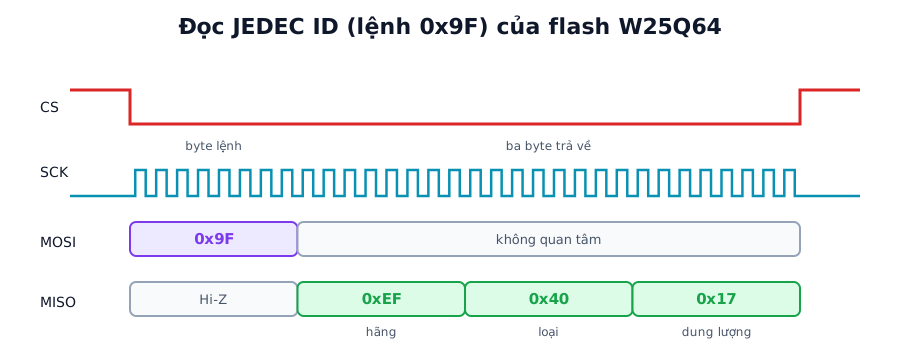
Figure 3. One ID read transaction. CS stays low throughout; the master sends one command byte and then 24 clock pulses to receive 3 bytes.
#define CS_LOW()   HAL_GPIO_WritePin(FLASH_CS_GPIO_Port, FLASH_CS_Pin, GPIO_PIN_RESET)
#define CS_HIGH()  HAL_GPIO_WritePin(FLASH_CS_GPIO_Port, FLASH_CS_Pin, GPIO_PIN_SET)

HAL_StatusTypeDef flash_read_id(uint8_t id[3])
{
    uint8_t cmd = 0x9F;
    CS_LOW();
    HAL_StatusTypeDef st = HAL_SPI_Transmit(&hspi1, &cmd, 1, 10);
    if (st == HAL_OK)
        st = HAL_SPI_Receive(&hspi1, id, 3, 10);
    CS_HIGH();
    return st;
}
If you read back 00 00 00 or FF FF FF, go through the fault table in section 6 before blaming the chip.
5.2. Reading, erasing and programming
Basic W25Qxx commands from the datasheet:
| Command | Code | Note |
|---|---|---|
| Write Enable | 0x06 |
Must precede every program or erase command |
| Read Status Register-1 | 0x05 |
Bit 0 is BUSY |
| Read Data | 0x03 |
Followed by a 24-bit address, then continuous data |
| Page Program | 0x02 |
Up to 256 bytes, must not cross a page boundary |
| Sector Erase (4 KB) | 0x20 |
Erase before writing; erased cells read 0xFF |
static void flash_wait_ready(void)
{
    uint8_t cmd = 0x05, st;
    do {
        CS_LOW();
        HAL_SPI_Transmit(&hspi1, &cmd, 1, 10);
        HAL_SPI_Receive(&hspi1, &st, 1, 10);
        CS_HIGH();
    } while (st & 0x01);              // BUSY
}

static void flash_write_enable(void)
{
    uint8_t cmd = 0x06;
    CS_LOW(); HAL_SPI_Transmit(&hspi1, &cmd, 1, 10); CS_HIGH();
}

void flash_read(uint32_t addr, uint8_t *buf, uint16_t n)
{
    uint8_t h[4] = { 0x03, addr >> 16, addr >> 8, addr };
    CS_LOW();
    HAL_SPI_Transmit(&hspi1, h, 4, 10);
    HAL_SPI_Receive(&hspi1, buf, n, 100);
    CS_HIGH();
}

void flash_sector_erase(uint32_t addr)
{
    uint8_t h[4] = { 0x20, addr >> 16, addr >> 8, addr };
    flash_write_enable();
    CS_LOW(); HAL_SPI_Transmit(&hspi1, h, 4, 10); CS_HIGH();
    flash_wait_ready();               // a sector erase takes tens to hundreds of ms
}

void flash_page_write(uint32_t addr, const uint8_t *data, uint16_t n)   // n <= 256, within one page
{
    uint8_t h[4] = { 0x02, addr >> 16, addr >> 8, addr };
    flash_write_enable();
    CS_LOW();
    HAL_SPI_Transmit(&hspi1, h, 4, 10);
    HAL_SPI_Transmit(&hspi1, (uint8_t *)data, n, 100);
    CS_HIGH();
    flash_wait_ready();
}
The Write Enable latch clears itself after every program or erase, so send 0x06 every time. Flash can only change bits from 1 to 0; getting back to 1 needs a sector erase, so only program areas that have been erased. Exact erase and program times are in the datasheet for your part.
5.3. Large transfers with DMA
static volatile uint8_t spi_done;

void HAL_SPI_TxRxCpltCallback(SPI_HandleTypeDef *hspi)
{
    if (hspi == &hspi1) spi_done = 1;
}

void HAL_SPI_ErrorCallback(SPI_HandleTypeDef *hspi)
{
    if (hspi == &hspi1) spi_done = 2;     // flag the error so the wait loop exits
}

int spi_xfer_dma(uint8_t *tx, uint8_t *rx, uint16_t n)
{
    spi_done = 0;
    CS_LOW();
    if (HAL_SPI_TransmitReceive_DMA(&hspi1, tx, rx, n) != HAL_OK) { CS_HIGH(); return -1; }
    while (!spi_done) { }                 // in practice use an RTOS semaphore or a non-blocking flag
    CS_HIGH();
    return (spi_done == 1) ? 0 : -1;
}
DMA has a setup cost, so for a few bytes polling is actually faster. It pays off from a few tens of bytes upwards, or when the CPU has other work to do during the transfer.
On parts with a data cache (STM32F7, H7), DMA buffers need cache maintenance: SCB_CleanDCache_by_Addr before sending and SCB_InvalidateDCache_by_Addr after receiving, or place the buffers in a non-cacheable region. The F1 and F4 have no data cache and need none of this.
6. Common faults
| Symptom | Usual cause | Fix |
|---|---|---|
| Reads all 0x00 | MISO pulled to GND, CS never asserted, slave unpowered | Probe CS and MISO with a logic analyzer, check power |
| Reads all 0xFF | MISO floating or pulled up, wrong CPOL/CPHA, wrong pin | Check the MISO wire, try modes 0 and 3 |
| Data shifted by one bit | Wrong CPHA or wrong bit order (MSB/LSB) | Compare against the mode table and the datasheet |
| Works slowly, fails fast | Long wires, noise, above the slave's maximum clock | Raise the prescaler, add series resistors, shorten wires |
| Last byte lost | CS released before the last byte has gone out | Wait for the SPI BUSY flag or the completion callback before CS_HIGH |
| Flash write changes nothing | Missing Write Enable or sector not erased | Send 0x06 before writing, erase the sector first |
| Two slaves interfere | Unselected slave's MISO not going Hi-Z | Check the datasheet, add a tri-state buffer |
7. When the STM32 is the SPI slave
The STM32 can also run as Full-Duplex Slave, with SCK and CS supplied by the master on the other side. In that role, enable hardware NSS so the chip knows when it is selected, and receive with DMA to keep up with the master.
A slave has no control over timing, so the first byte from the master usually arrives before the firmware has a reply ready. The protocol between the two sides therefore needs a padding byte at the start, or a separate "ready" line. This will get its own measurement article.
8. Measurement plan
The "Measured" column stays empty until the code runs on hardware.
| Test | Method | Calculated | Measured |
|---|---|---|---|
| SCK frequency with prescaler 8 | Logic analyzer or oscilloscope | 10.5 MHz (84 MHz bus) | (to be filled) |
| The four SPI modes | Read the JEDEC ID in all 4 modes, note which work | Expected to work in modes 0 and 3 | (to be filled) |
| Time to read 4 KB, polling | Toggle a GPIO around flash_read, measure with a logic analyzer |
3.12 ms at 10.5 MHz (clock only) | (to be filled) |
| Time to read 4 KB, DMA | As above, compare with polling | Close to polling, CPU free | (to be filled) |
| Gaps between bytes when polling | Logic analyzer, measure the gap between consecutive bytes | None if one multi-byte call is used | (to be filled) |
| Highest speed that reads correctly | Raise SCK step by step, verify the data | Depends on wiring and chip | (to be filled) |
| Effect of wire length | Oscilloscope on SCK edges and ringing | Depends on wiring | (to be filled) |
9. FAQ
How much faster is SPI than I²C? Counting clock alone, SPI at 10 MHz is about 25 times faster than I²C Fast mode (400 kHz). Real numbers depend on the firmware.
Does SPI need pull-up resistors? Usually not, because the SPI lines are push-pull. The exception is CS: a pull-up keeps the slave from being selected by accident while the MCU is in reset.
Should I use hardware NSS as master? In most cases driving CS from a GPIO is simpler and more flexible, especially with several slaves or when one transaction has to keep CS low across several HAL calls.
HAL_SPI_TransmitReceive, or Transmit followed by Receive? Both work. Receive in Full-Duplex Master mode still clocks out dummy bytes on its own. When a chip expects a particular dummy byte (0xFF, for example), use TransmitReceive with a transmit buffer you fill yourself.
Summary
Read the datasheet to set CPOL/CPHA correctly, release CS only after the last byte has gone out, and start at a low clock rate. Those three habits cover most SPI problems.
Part 3 moves on to I²C: fewer wires, addressing and ACK, but also pull-up resistors and the occasional stuck bus.
To check data read back from the flash, try the Capitlab Hex Converter and CRC calculator.
References
- Winbond W25Q64/W25Q128 datasheet (command table, JEDEC ID, erase and program times)
- The reference manual for your STM32 (SPI chapter) and the STM32 HAL documentation (
HAL_SPI_*functions)